April 26, 2024
Black phosphorus (BP), also known as phosphorene, is catching the attention of many scientists as a promising layered two-dimensional (2D) material for electronic, optoelectronic, and thermoelectric applications. Compared to its red and white counterparts, black phosphorus is the most thermodynamically stable allotrope of phosphorus and is derived by heating its white counterpart under extremely high pressure.
Similar to its more famous 2D peer, graphene, phosphorene has unparalleled properties, including high hole mobility and a tunable bandgap. These properties lead researchers to investigate BP as a potential thermoelectric material.

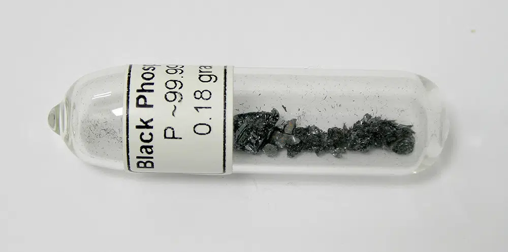
Figure 1. Black Phosphorus. Credit: Berkeley Lab
Black phosphorus (BP) has gained considerable attention in recent years due to its unique physiochemical properties. BP possesses a strong, unique, puckered honeycomb-layered structure that gives rise to its distinctive properties.
Graphene, the most represented 2D material, shares many properties with phosphorene, such as high thermal conductivity, carrier mobility, and chemical stability. Graphene lacks phosphorene’s thickness-dependent bandgap from 0.3-2.0 eV. A bandgap refers to the energy difference between the valence band’s highest energy level and the conduction band’s lowest energy level. A bandgap represents the minimum energy required to excite an electron up to a state in the conduction band where it can participate in electrical conduction. This bandgap’s existence and size determine whether the material will act as an electrical conductor, semiconductor, or insulator.
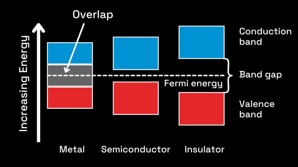
Figure 2. The band gap diagram shows the band gap sizes for conductors, semiconductors, and insulators.
The tunable bandgap of BP causes the material to act as a semiconductor, allowing its electrical conductance to switch on and off, a crucial characteristic of materials used in the electronic industry. This band gap also allows for a large photon absorption window, implying a strong energy conversion process potential.
In 2015, researchers at the US Department of Energy’s National Lawrence Berkeley Laboratory discovered that single-crystal black phosphorus nanoribbons display strong anisotropic in-plane thermal conductivity.
Lawrence Berkeley National Laboratory researchers utilized a top-down approach to synthesize black phosphorus nanoribbons. The measurements were carried out in steady-state longitudinal heat flow using suspended micro-pad devices. The nanoribbons were thermally isolated before measurement to ensure the slight temperature gradient and thermal conduction could be accurately determined.
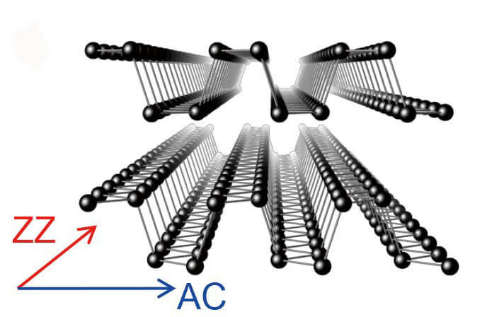
Figure 3. Illustration from the Berkeley Lab showing the directions of measurement of in-plane thermal conductivity of black phosphorus. Credit: Berkeley Lab
The results of this study explain how heat flow in the black phosphorus nanoribbons can be extremely different along the different directions in-plane. The atomic arrangement of each layer of BP produces two distinct directions along the zigzag (ZZ) and the vertical armchair (AC) type structures (Figure 3). Through detailed analysis, researchers at the Lawrence Berkeley National Laboratory concluded the anisotropy in the thermal conductivity originates from phonon dispersion and the phonon-phonon scattering rate. Before this study, the thermal conductivity anisotropy of 2D BP had only been predicted and never before observed.
This research reveals the intrinsic orientation-dependent thermal conductivity of black phosphorus. The implications of this discovery are enormous for the development and design of electronics and optoelectronics, as it indicates that thermal and electrical conductivities have opposite anisotropy. The authors emphasize that with such anisotropy in the thermal conductivity of black phosphorus nanoribbons, be sure to consider orienting the layered material in patterns specific to their desired application. This pattern of anisotropy is highly advantageous for applications where heat generation and dissipation play crucial roles in the operation of the device. As Junqiao Wu, one of the corresponding authors of this research paper, puts it:

Figure 4. Quote from Junqiao Wu.
The opposite anisotropy of electrical and thermal conductivities allows devices made with the material to powerfully conduct electricity while dissipating heat quickly, making them more efficient. This discovery is critical for developing high-performance electronic, optoelectronic, and thermoelectric devices using phosphorene. The results of this study also play a prominent role in understanding the fundamental physical properties of layered materials within the few- or monolayer limit.
Black phosphorus is emerging as a promising material for the future of electronic, thermoelectric, and optoelectronic devices. BP is an exceptionally thin 2D material, a property that makes this material suitable for developing smaller, more flexible electronic devices.
Recent research shows that black phosphorus could potentially replace silicon as the primary material used in electronic devices. BP has higher charge carrier mobility than silicon, meaning it can carry electrical charge more efficiently. Silicon also lacks the tunable band gap found in BP. This band gap allows the material to switch its electrical conductance on and off, acting as a semiconductor. This property opens the doors for future applications of black phosphorus in imaging tools, night vision devices, and other optoelectronic applications. BP is smaller than silicon, reducing electronic device size limitations.
The controllable bandgap in black phosphorus also potentiates its use as a topological insulator. These materials can act as insulators on the inside and a conductor on their surface. Topological insulators have promising applications in developing low-power electronics to prevent electron scattering on their surface.
Current applications of black phosphorus include secondary battery systems, where BP serves as both the negative and positive electrode material for batteries, allowing for the storage of electricity from unstable sources such as wind turbines and solar panels. BP is also used for the construction of flexible, cost-effective, and high-performance supercapacitor devices. It has even been proven to be an efficient photo- and electrocatalyst in energy conversion processes such as carbon dioxide conversion, water splitting, and nitrogen reduction.

Figure 5. Industries that benefit from the use of Black Phosphorus.
Black phosphorus is a promising material for future electronic, optoelectronic, and thermoelectric applications due to its unique properties, tunable bandgap, and anisotropic in-plane thermal conductivity. The recent discovery of the intrinsic orientation-dependent thermal conductivity of BP nanoribbons opens new avenues for designing high-performance devices that can efficiently conduct electricity while dissipating heat, making them much more energy-efficient. With its potential to replace silicon in electronic devices and its applications in various fields such as energy storage, catalysis and optoelectronics, black phosphorus is poised to play a significant role in shaping the future of electronics.
Further research is needed on the scalability, quality, and stability of black phosphorus for future energy storage and conversion processes to fully harness its potential. BP’s intriguing properties open exciting opportunities for potential applications in various fields.
Read the research paper published by the team in Nature Communications.
Black phosphorus (BP) is the most stable allotrope of phosphorus. It is most commonly synthesized by heating white phosphorus, another allotrope, under extreme temperature and pressure. The puckered honeycomb lattice of the crystal structure gives rise to incredible carrier mobility. BP, while being very similar to graphite, possesses a tunable bandgap and demonstrates remarkable in-plane anisotropy, making it an ideal candidate for electronic, thermoelectric, and optoelectronic applications.
Anisotropic in-plane thermal conductivity refers to a phenomenon in which the thermal conductivity of a material varies depending on the direction within the plane of the material. This is due to the material’s unsymmetrical atomic structures along different axes. Materials classified as anisotropic can have significant differences in their thermal conductivity values between in-plane directions.
A bandgap refers to the energy difference between the highest occupied (valence) energy band and lowest unoccupied (conduction) energy band. The bandgap is representative of the minimum energy required to excite an electron into the conduction band, where it can participate in electrical conduction. The existence and size of the bandgap is what determines whether a material will act as a conductor, semiconductor, or insulator.
The discovery that the electrical and thermal conductivities of black phosphorus have opposite anisotropy has major implications for the future of electronic and optoelectronic design. This opposite anisotropy indicates devices made with BP would not only effectively conduct electricity, but it would also dissipate heat quickly. A crucial feature to electronic design, making the device more efficient overall. For the electronics world, this discovery could lead to the creation of much smaller, more flexible devices that can efficiently conduct electricity while preventing overheating.
Silicon is one of the primary materials used in electronic design but could soon be replaced by black phosphorus in certain electronic applications. With the quest for ever smaller electronic devices coming to its limit, BP is becoming a more favorable semiconductor, as it can be layered down to just a few atomic layers, allowing for smaller more flexible electronic devices.
Black phosphorus also exhibits a higher charge mobility than silicon and possesses a tunable bandgap making this material a promising upgrade to silicon in various electronic applications.
Deng, B., Tran, V., Xie, Y., Jiang, H., Li, C., Guo, Q., Wang, X., Tian, H., Koester, S. J., Wang, H., Cha, J. J., Xia, Q., Yang, L., & Xia, F. (2017). Efficient electrical control of thin-film black phosphorus bandgap. Nature Communications, 8(1). https://doi.org/10.1038/ncomms14474
Kulkarni, A. A., Gaikwad, N. K., & Bhat, T. S. (2023). Black phosphorus: Envisaging the opportunities for Supercapacitors. Journal of Electroanalytical Chemistry, 942, 117543. https://doi.org/10.1016/j.jelechem.2023.117543
Lee, S., Yang, F., Suh, J., Yang, S., Lee, Y., Li, G., Sung Choe, H., Suslu, A., Chen, Y., Ko, C., Park, J., Liu, K., Li, J., Hippalgaonkar, K., Urban, J. J., Tongay, S., & Wu, J. (2015). Anisotropic in-plane thermal conductivity of black phosphorus nanoribbons at temperatures higher than 100 K. Nature Communications, 6(1). https://doi.org/10.1038/ncomms9573
Li, P., Lu, J., Cui, H., Ruan, S., & Zeng, Y.-J. (2021). The development, application, and performance of black phosphorus in energy storage and conversion. Materials Advances, 2(8), 2483–2509. https://doi.org/10.1039/d0ma01016b
Yarris, L. (2015, October 21). Is black phosphorous the next big thing in materials? – berkeley lab. Berkeley Lab News Center. https://newscenter.lbl.gov/2015/10/16/is-black-phosphorous-the-next-big-thing-in-materials/